
As you hear the phrase "stacked chips", you may be thinking about a snack.

It might bring to mind the stacked potato-based chips that Procter & Gamble (P&G) invented in 1968. Fun fact: Each Pringles chip is in the mathematical shape of a hyperbolic paraboloid; which may be described as a doubly ruled surface containing two families of mutually skew lines; two lines in three-dimensional space that are not parallel, do not intersect, and are not coplanar.
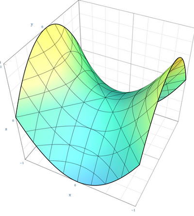
The lines in each family are parallel to a common plane, but not to each other. Hence the hyperbolic paraboloid is a conoid; a type of ruled surface where all the generating lines intersect a fixed line (axis) and are parallel to a specific plane (directrix plane), which aligns with the definition of a conoid. Actually, the hyperbolic paraboloid is doubly a conoid; more precisely, it is a conoid with axis one of the lines, directrix plane (P') and directrix another line, and a conoid with axis one of the lines, directrix plane (P) and directrix another line.

Hopefully, the preceding-misleading introduction had a light humorous effect. Admittedly, these high-rise stacked chips aren't the kind seen within the city. Nor are they the kind that you should not be thinking about in between meals. Actually, they are completely unrelated to skyscrapers and popular snacks. They are of the technical variety. Once they are successfully commercialized, they may improve AI hardware efficiency in foreseen and unforeseen ways.
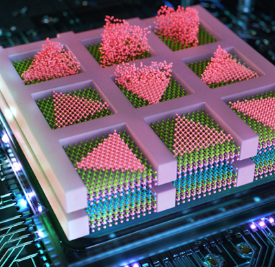
These are stacked 3D computer chips that utilize a growth-based monolithic 3D integration technique, which stacks the single-crystal 2D semiconductors. The technology behind the 3D chip innovation, which could increase the number of transistors, relies on the use of two-dimensional (2D) materials; involving transition metal dichalcogenides, which are also known as TMD’s, grown at relatively low temperatures; a class of thin and layered materials; made of transition metals and chalcogen atoms; the group of elements including sulfur (S), selenium (Se), tellurium (Te), polonium (Po), and livermorium (Lv) clustered to form compounds with electropositive elements.
A chemical formula of (MX_{2}), where (M) is a transition metal and (X) is a chalcogen atom, allows for the seamless stacking of multiple layers without damaging the underlying components. It is a process that involves growing atomically thin layers of TMDs directly on top of each other, using a technique called remote epitaxy, in order to transfer these layers onto a silicon wafer, which incorporates vertical electrical connections between each of the layers for the purpose of laying the foundation; the bedrock for efficient data transfer.

What exactly is it that makes this particular approach such an innovative one? Essentialy, it overcomes limitations of traditional silicon-based 3D integration requiring high temperatures that can damage underlying circuits. By utilizing 2D materials, a scalable method for producing high-performance, densely packed 3D chips that can double processing power while maintaining the same footprint as current designs has been created. Scalability and power efficiency, address key challenges in modern computing. The vertical stacking of these transistors should allow for a dramatic increase in transistor density.
As limitations of 2D chip designs reach physical miniaturization constraints, enhanced scalability of 3D computer chips transcends limitations. Obviously, these AI applications require a considerable amount of computational power. Enabling more transistors to be packed into a given area, the technology, when it's further developed, could lead to the development of AI hardware that is not only more powerful but also more energy-efficient. Efficiency gains are critical for reducing data center's carbon footprints as it enables more sophisticated AI models to run on edge devices with limited power resources.
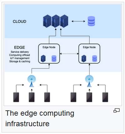
Edge computing is a distributed computing model that brings computation and data storage closer to the sources of data. It refers to the design, which pushes computation physically closer to the user in order to reduce latency; compared to when an application typically runs on a centralized data center.
Compact and energy-efficient design power more sophisticated AI models on mobile devices and IoT sensors, which enables real-time decision-making while reducing reliance on cloud processing. Integrating logic and memory components in these 3D structures could reduce data transfer bottlenecks and enhance system performance for AI and computationally intensive tasks. Increased transistor density combined with improved processing power of these high-rise, stacked 3D chips make them ideally suited for AI workloads.

These types of advancements could enable more efficient implementation of neural networks and in the process accelerate important tasks such as machine learning, computer vision, and natural language processing that are likely to have far-reaching, near-future implications for AI-driven technologies.
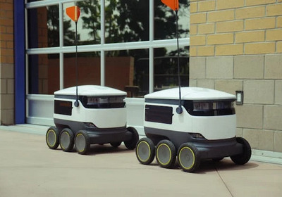
Autonomous vehicles (also known as self-driving cars, driverless cars, robo-taxis and robotic-cars) are capable of operating with reduced or without human input. They are responsible for the broad range of driving activities, such as perceiving the environment, monitoring its systems and controlling the vehicle; a process that includes navigating from origin to destination. Improved on-board AI processing could enhance its self-driving capabilities, its efficienty for object recognition, and its thoroughness for route optimization.
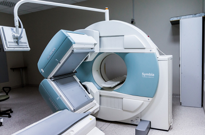
Medical imaging is the technique and process of imaging the interior of a body for clinical analysis and medical intervention, as well as visual representation of the function of some organs or tissues (physiology). Medical imaging seeks to reveal internal structures hidden by the skin and bones, as well as to diagnose and treat disease. Medical imaging also establishes a database of normal anatomy and physiology to make it possible to identify abnormalities. Although imaging of removed organs and tissues can be performed for medical reasons, such procedures are usually considered part of pathology instead of medical imaging. Faster and more accurate analysis of medical scans and diagnostic data could be achieved that improves patient outcomes.

Financial modeling: the task of building an abstract representation (a model) of a real world financial situation. This is a mathematical model designed to represent (a simplified version of) the performance of a financial asset or portfolio of a business, project, or any other investment. High-speed processing of complex financial algorithms and risk assessments could be facilitated resulting in more informed decision-making in the finance sector. As these 3D chips move from the laboratory to commercial production, they’re expected to drive advancements in AI hardware, which could potentially unlock new possibilities in fields ranging from robotics to climate modeling.

A spinout company has been recently formed for the express purpose of building the true 3D chips using 2D materials. As this tech moves towards commercialization with support from academic and industry partners confident its potential to revolutionize the semiconductor industry by way of enabling more efficient AI hardware and compact electronics, development has garnered attention from major players within the tech industry, who recognize that its can address the growing demand for more powerful and energy-efficient computing solutions. Once it is further developed, its applications are anticipated in various field such as consumer electronics, data centers, and specialized AI hardware. It can reshape the landscape of the semiconductor industry and accelerate the development of next-generation AI systems.

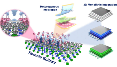
Why exactly are these advanced heterogeneous integration technologies considered pivotal for next-generation electronics? Essentially because they’re single-crystalline materials, which is one of the key building blocks for heterogeneous integration. Although, producing and then integrating these materials is undoubtedly a daunting task. However there is a practical solution available for growing single-crystalline thin films exfoliated from host wafers and transferred onto foreign platforms. That solution is called Remote epitaxy!

This is an ambitious venture poised to revolutionize AI hardware applications across its various domains. This technology has garnered attention for its application for materials, functionalities and novel application platforms. However, remote epitaxy, an emerging technology for producing single-crystalline, free-standing thin films and structures, is a delicate process. Subsequently, its successful execution is not without its share of challenges.
Clarifying the collective mechanisms involved, summarizing its breakthroughs, discussing its challenges, devising solutions, forecasting future applications, evaluating the fundamentals and functions of this emerging materials science and improving production techniques are all key components in this venture; each of the above will ultimately determine the level of its inevitable success.
Floor Covering Media publishes
blog articles called Flooring Briefs.

Floor Covering Media is
a social media network.

Retrieve timely, objective news and
information at https://www.floorsearch.info.